
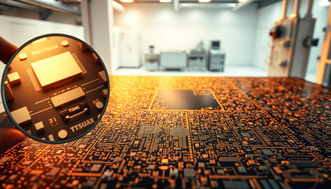
TSMC's 2nm Wafers: The Next Big Step in Semiconductor Tech
Taiwan Semiconductor Manufacturing Company (TSMC) is leading the way with its 2nm wafers. This move in semiconductor advancement is set to change the game in chip making. It will bring us chips that are not just smaller and faster but also use less energy.
The TSMC 2nm technology is a big step forward in advanced wafer technology. It's going to make a huge difference in our daily lives, from smartphones to AI systems.
Key Takeaways
- 2nm wafers represent a major shift in semiconductor design and manufacturing.
- TSMC leads global efforts to advance next-gen chip production at 2nm scale.
- This technology reduces power consumption while boosting device performance.
- It enables thinner smartphones, faster data centers, and smarter IoT devices.
- Mass production of advanced wafer technology could reshape industries by 2025.
Understanding the Breakthrough: What Are 2nm Wafers?
Advances in 2nm semiconductor technology are changing electronics. Let's explore what this means and why it's important.
The Evolution of Semiconductor Node Sizes
Chips have shrunk from 90nm in the 2000s to today's 3nm. This semiconductor evolution is a race to make things smaller. Each size reduction adds more power in less space.
Early 7nm and 5nm nodes changed smartphones and servers. Now, 2nm takes it even further.
How 2nm Technology Differs from Current Standards
Going from 3nm to 2nm is more than just smaller sizes. The nanometer node size comparison shows a big design leap. Traditional FinFET transistors are replaced with gate-all-around (GAA) structures.
This change lets circuits be closer without losing speed or heat control.
Key Technical Advantages of 2nm Process
These wafers bring three big benefits:
- Higher transistor density—fitting 1.6 times more transistors than 3nm
- Lower power consumption for longer device battery life
- Enhanced computational speeds for AI and high-performance computing
These upgrades mean smaller chips can do complex tasks better than ever.
TSMC's Journey to 2nm Innovation
Since its start, TSMC has led the way in making chips smaller. Their TSMC technology roadmap shows years of semiconductor R&D and constant chip fabrication innovation. They moved from 7nm in 2018 to 5nm in 2020, setting the stage for today's 2nm breakthrough.
| Technology Node | Year Launched | Key Breakthrough |
|---|---|---|
| 7nm | 2018 | First mass production of EUV lithography |
| 5nm | 2020 | 50% performance boost over 7nm |
| 3nm | 2022 | Nanolaminate channel material adoption |
These achievements come from huge investments in R&D and top-notch facilities. Engineers tackled big challenges like controlling defects at the nanoscale and improving energy efficiency. C.C. Wei, TSMC’s co-CEO, said:
“Every node transition requires reinventing manufacturing physics.”
From 2018 to now, TSMC’s TSMC manufacturing milestones clearly show the path to 2nm. It's not just about making things smaller. It's about staying ahead through careful innovation. With each step, they've perfected processes that now allow for 2nm. The journey continues, but past achievements give hope for future successes.
TSMC Mass Production 2nm Wafers: Timeline and Roadmap
Every breakthrough needs a solid plan. TSMC’s 2nm wafer availability is based on a detailed semiconductor manufacturing timeline. This part explains the chip fabrication roadmap and important dates for the TSMC 2nm production schedule.
Initial Research and Development Phase
Research started in 2018, focusing on tiny transistor design. Key milestones include:
- 2020: Early transistor prototypes finished
- 2022: Material science breakthroughs finalized
- 2023: Process node validation with industry partners
Current Production Status
Pilot production facilities in Tainan, Taiwan are now up and running. As of Q2 2023:
| Phase | Status |
|---|---|
| R&D | Completed core innovations |
| Pilot Runs | Testing 1,000+ wafers monthly |
| Customer Collaboration | Early samples sent to leading tech firms |
Full-Scale Manufacturing Projections
By 2025, TSMC plans to start risk production. Full-scale manufacturing goals include:
“Volume production depends on resolving final yield rate challenges.”
Key milestones ahead:
- Risk production starts mid-2025
- Initial customer sampling by end-2025
- Mass production capacity reaches 10,000+ wafers/month by 2026
These steps ensure 2nm wafer availability meets global demand while keeping quality high.
Technical Specifications: Inside the 2nm Process
TSMC’s 2nm process is a game-changer in chip design. It brings new transistor designs and better power management. Let's explore how these advancements will shape future devices.
Gate-All-Around Transistor Architecture
The heart of TSMC’s 2nm process is the Gate-All-Around transistors. This design wraps the gate around the channel, making transistors smaller and faster. It also cuts down on electrical leakage and boosts control at the atomic level.
- Wraps the gate electrode around the semiconductor channel
- Enables scaling to 2nm without sacrificing performance
- Improves signal integrity for higher clock speeds
“The Gate-All-Around design is the critical enabler for 2nm—no other architecture can deliver this precision at this scale.” — TSMC Technical Briefing
Semiconductor Power Efficiency Improvements
Power savings are a major focus. TSMC boasts semiconductor power efficiency gains of up to 30% over 3nm nodes. This means:
- Longer battery life for smartphones
- Lower cooling needs for servers
- Less energy costs for data centers
2nm vs 3nm Performance Metrics
Quantitative advancements highlight 2nm's superiority. Here's a comparison:
| Node Size | Transistor Density | Performance Boost | Power Reduction |
|---|---|---|---|
| 2nm | 250 million/cm² | +15% speed | 25-30% lower voltage |
| 3nm | 173 million/cm² | +11% over 5nm | 20% reduction |
| 5nm | 100 million/cm² | Baseline standard | Previous industry leader |
These improvements come from chip architecture advancements like EUV lithography and nanosheet structures. The outcome? Chips that perform better, faster, and use less power than ever.
Market Impact: Industries Set to Benefit
2nm chip applications are set to change how industries work. The impact on the semiconductor industry will be huge. Companies will use smaller, faster chips in many areas. This will lead to big upgrades in technology sectors.
- Smartphones: Next-gen devices could last days on a single charge. They will run AI-driven features like real-time language translation or advanced photography.
- Artificial Intelligence: AI systems will process data faster. This will lead to breakthroughs in healthcare diagnostics and autonomous systems.
- Automotive: Self-driving cars will make better decisions. This is because chips can handle complex sensor data.
- Data Centers: Servers using 2nm chips could cut energy use by up to 30%. This will lower operational costs for cloud services.
| Industry | Application | Impact |
|---|---|---|
| Consumer Electronics | Smartphones/tablets | Thinner designs with extended battery life |
| AI/ML | Machine learning models | Faster training and inference times |
| Automotive | Autonomous driving systems | Improved real-time object detection |
| Data Centers | Cloud infrastructure | Enhanced scalability and efficiency |
“2nm technology isn’t just a step forward—it’s a leap into new product categories we can’t even imagine yet,” said a TSMC spokesperson discussing 2nm chip applications at a recent tech summit.
Big names like Apple and NVIDIA are already using these chips in prototypes. The impact on the semiconductor industry will create a big demand for skilled workers and R&D investment. As production grows, we will see real improvements in how devices work and their environmental impact.
The Competitive Landscape: How TSMC Leads the Pack
As TSMC moves towards 2nm production, the semiconductor industry competition gets fiercer. Intel and Samsung are racing to keep up with TSMC's pace. This section looks at how big players are reacting and why TSMC stays ahead.
“The race to 2nm isn’t just about speed—it’s about who can balance cutting-edge tech with reliable mass production.” — Semiconductor Industry Analyst

Intel's Response to 2nm Development
Intel is under a lot of pressure in the Intel vs TSMC battle. TSMC plans to release 2nm chips by 2025. Intel is working on its 20A/20B process, using RibbonFET transistors, to catch up. But, delays in US factory builds and yield rate issues are causing problems.
Intel is now looking at working with external foundries as part of its strategy.
Samsung Foundry Services and Competing Technology
Samsung is also in the game with its 2nm GAA (Gate-All-Around) tech, set for 2024. Samsung Foundry Services has won contracts with companies like Qualcomm. But, TSMC's experience in mass production and cost efficiency keep it in the lead.
Global Manufacturing Capabilities Comparison
Why do only a few companies lead? TSMC's success comes from:
- Advanced process control and R&D investment
- Decades of chip manufacturing leadership experience
- Access to specialized equipment and supply chains
Samsung and Intel are trying hard, but TSMC's 2nm achievements show its dominance in thesemiconductor industry competition.
Economic Implications of Advanced Semiconductor Production
Advancing to 2nm technology changes the world economy. It affects industries and jobs in big ways.
Investment Requirements for 2nm Facilities
Creating 2nm facilities needs huge chip manufacturing investment. TSMC’s Arizona plant, for example, costs over $20 billion. These costs include top-notch tools like EUV lithography systems.
These costs are very high. Governments like the U.S. are giving subsidies to help with these costs.
High-Tech Job Creation Needs
Advanced fabs create lots of high-tech jobs. There are three main areas:
- Engineers who design at the nanoscale
- Technicians who work with AI in production
- Material scientists who handle ultra-pure silicon
Most jobs need at least a bachelor’s degree. But 40% require a master’s degree.
Technology Supply Chain Challenges
The global technology supply chain is under pressure. It needs raw materials like hafnium and special chemicals. But these come from unstable regions.
There are also equipment shortages from companies like ASML and Lam Research. This makes production harder. U.S. policies try to make supply chains more local to reduce Asian dependence.
Future Applications: What 2nm Will Enable
2nm wafers are more than just smaller chips. They open doors to future technology applications that were once dreams. Think of AI systems that process data instantly or smartphones that last days on a single charge. These leaps are thanks to TSMC’s 2nm innovation, which breaks new ground in power and speed.
- AI computing advancement: With smaller nodes, neural networks can work faster. This means companies like NVIDIA and Google can create AI models that run on devices, not just in the cloud.
- Next-gen mobile devices: We can now make phones that are thinner and last longer. Apple's new iPhones and Samsung's foldables might use 2nm chips for better multitasking and streaming 4K videos.
- Healthcare: Wearables with 2nm sensors could track vital signs in real time. This could help detect diseases early.
| Technology | Current Limitation | 2nm Potential |
|---|---|---|
| Autonomous vehicles | Slow sensor processing | Real-time obstacle detection at 99% accuracy |
| AR headsets | Heavy battery use | 8-hour battery life for immersive experiences |
These chips could change many industries. For example, self-driving cars need to process data fast to avoid accidents. 2nm makes that possible. Also, semiconductor innovation impact will be huge in IoT, where billions of devices need efficient chips. This is not just progress; it's a big step towards smarter, greener tech.
Challenges and Hurdles in 2nm Production
Going to 2nm production is a big step forward. But it also brings new risks. Engineers face semiconductor manufacturing challenges that push current tech to its limits.
Technical Manufacturing Challenges
Some major hurdles include:
- Low initial chip production difficulties due to nanoscale imperfections
- Lithography systems pushing ultraviolet light tech to extremes
- Material instability at atomic scales
Economic Viability Concerns
Advanced node economics raise big questions:
| Factor | Impact |
|---|---|
| R&D Costs | $20B+ per fab investment |
| Yield Rates | Higher waste rates early on |
| Market Demand | Uncertain adoption timelines |
Geopolitical Factors
"Taiwan’s position creates strategic risks for global supply chains." – Semiconductor Industry Association 2023 Report
Geopolitical semiconductor issues are a big concern. TSMC’s Taiwan factories face tension between China and the US. Export controls and tech embargoes could mess up shipments to key markets.
To overcome these challenges, we need to balance innovation with reality. Solutions require teamwork across industries and governments. We must work together to explore this new frontier.
Conclusion: TSMC's 2nm Technology and the Future of Computing
TSMC's 2nm wafers are a huge step forward in the semiconductor industry future. They push computing technology advancement to new heights. These chips will be faster and more efficient, changing everything from phones to data centers.
By making transistors smaller than atoms, TSMC is not just improving current tech. It's creating next-generation processors for AI, self-driving cars, and medical devices. This could lead to major breakthroughs.
The chip innovation impact goes beyond the lab. Soon, we'll have thinner gadgets that last longer. Healthcare and cars will get better tools to solve big problems. But, there are hurdles like high costs and supply chain issues.
TSMC plans to start mass production by 2025. But, how fast it gets to our devices depends on cost and demand. It's a delicate balance.
For those not into tech, this means better gadgets sooner than we thought. TSMC is racing with Samsung and Intel to make smaller chips. This race drives tech forward, making our lives better.
TSMC's 2nm milestone is more than just a factory achievement. It shows us the future of computing is coming, one nanometer at a time.
FAQ
What makes TSMC's 2nm wafers different from earlier technologies?
TSMC's 2nm wafers use a new transistor design. This design boosts performance and power efficiency. It also packs more transistors into a smaller space than before.
When is TSMC expected to begin mass production of 2nm wafers?
TSMC is already starting pilot production. They plan to start full production soon. They have set milestones for risk production and initial customer sampling.
How will 2nm technology impact everyday consumers?
Consumers will see big improvements. Smartphones will last longer, and AI will work faster. Devices will get more powerful while using less energy.
What challenges does TSMC face in developing 2nm technology?
TSMC faces technical and economic hurdles. They must manage yield and cost. Geopolitical tensions also pose a risk to production.
Which industries will benefit the most from 2nm technology?
Smartphones, automotive tech, and data centers will see big gains. Companies like Apple and AMD are already working on 2nm products.
How does TSMC's 2nm technology influence the competitive landscape?
TSMC's lead pushes Intel and Samsung to innovate. With limited global manufacturing, TSMC stays ahead by adopting new tech.
What are the broader economic implications of TSMC's R&D for 2nm technology?
TSMC's investment will create jobs in tech. It will also boost local economies and affect the global supply chain.
Comments
Post a Comment